Reverse Engineering PCB Solutions for Canton Fair 2026?

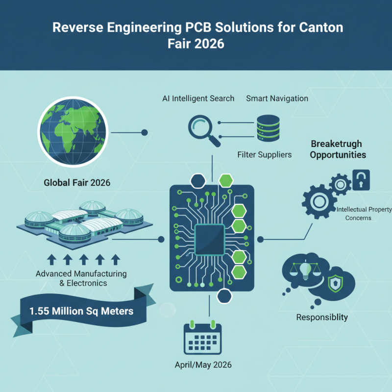
The Canton Fair 2026 promises to be a dynamic event, drawing global attention with its focus on advanced manufacturing and electronics. Reverse Engineering Pcb solutions will be a vital topic of interest for attendees. This year, over 1.55 million square meters of exhibition space will highlight the latest innovations.

With advancements like AI intelligent search and smart navigation, navigating this expansive venue will be more efficient. Buyers can filter suppliers based on specific qualifications. It's an exciting leap forward, yet the challenge remains to adapt to these technologies.

Reverse Engineering PCB may offer breakthrough opportunities but also raises concerns about intellectual property. Attendees must ponder the ethical implications while exploring these advanced technologies. The balance between innovation and responsibility is crucial as we approach this massive gathering in April and May 2026.

Reverse Engineering PCB Solutions for Canton Fair 2026?

Understanding PCB Reverse Engineering Techniques

Reverse engineering PCB solutions plays a crucial role in the electronics manufacturing industry. Techniques often involve designing a circuit board to understand its components and functionality. Detailed imaging and inspection methods, like X-ray analysis, provide insights into the layered structures of PCBs. These methods help in understanding how to replicate or modify existing designs.

One common technique is circuit extraction. It reveals connections between components. This can be challenging due to the complexity of modern PCBs. Often, mistakes occur during this process, leading to incomplete or inaccurate data. Engineers need to remain vigilant in their analysis, as small oversights can lead to significant issues later.

Another vital technique is component analysis. Identifying the specifications of each part is essential. This includes understanding the materials used and their capabilities. However, every board presents unique challenges. Intricate designs can confuse even seasoned professionals. Continuous reflection on these methods can enhance future reverse engineering efforts, driving innovation in PCB development.

Reverse Engineering PCB Solutions for Canton Fair 2026

Technique Description Application Benefits
X-Ray Inspection Utilizes X-ray imaging to analyze internal structures. Quality control, defect analysis Non-destructive, detailed view of assembly
3D Scanning Captures 3D data of the PCB for detailed study. Reverse engineering, prototyping Accurate physical representation, quick modification capabilities
Circuit Decapsulation Removes encapsulation to access semiconductor chips. Component analysis, IP verification Direct access to silicon, reveals proprietary designs
Signal Integrity Analysis Evaluates signal degradation in the PCB layout. Design optimization, debugging Improves performance, minimizes error rates

Key Tools and Technologies for PCB Analysis

In the realm of PCB analysis, several essential tools facilitate reverse engineering processes. One crucial tool is the optical microscope. It provides a close-up view of component layouts. This analysis allows engineers to identify design patterns and trace connections effectively. Often, details are missed by the naked eye. A robust microscope reveals them clearly.


Another key technology is X-ray imaging. This tool allows technicians to inspect internal layers without damaging the board. X-rays can reveal hidden vias and solder joints. Such insights are invaluable during PCB troubleshooting. Yet, precision matters immensely. Poor imaging can lead to incorrect assumptions and costly errors.


Software solutions are also vital. Tools that analyze schematics or layouts help in understanding circuit behavior. They aid in simulating how the PCB will perform. However, software complexity can be daunting. Users often struggle to navigate advanced features. This factor can hinder effective analysis, demanding ongoing learning and adaptation.

Analyzing Market Trends for PCB Solutions at Canton Fair 2026

As the Canton Fair 2026 approaches, market trends in PCB solutions are becoming increasingly vital. The need for efficient and cost-effective PCB designs is evident. Many manufacturers are exploring innovative methods to meet evolving demands. Specifically, reverse engineering stands out. This method allows companies to analyze existing products. It unveils key features that enhance performance or reduce costs.

However, not all reverse engineering efforts yield successful results. Some companies may overlook critical design elements. This can lead to ineffective solutions that fail to meet market expectations. Furthermore, understanding local preferences is essential. Designers must adapt to regional requirements, which often vary drastically. Inadequate research could result in products that don't resonate with consumers.

In this rapidly evolving landscape, staying abreast of emerging technologies is crucial. Sustainability and energy efficiency are becoming priorities. Yet, many industry players still struggle with these issues. Embracing these changes is necessary for competitive advantage. However, it also requires a willingness to learn from past mistakes and failures. The journey ahead is challenging but essential for growth.

Best Practices for Reverse Engineering in Electronics

Reverse engineering in electronics has become a vital practice, especially for upcoming events like Canton Fair 2026. This technique allows professionals to analyze existing designs, uncover underlying principles, and create new innovations. By understanding the intricacies of PCBs, experts can enhance product efficiency and functionality.

When embarking on reverse engineering, proper techniques are crucial. Take meticulous notes during your analysis. Document every component and its placement. Recognizing patterns helps streamline the process. Utilize software tools that assist in schematic capture. They can reveal connections that are not immediately obvious.

Tips: Always consider the ethical implications of reverse engineering. Steer clear of direct duplication. Instead, aim for inspiration and improvement. Collaborate with others for diversity in problem-solving. Often, insights from different fields can spark innovative ideas. Adjust your approach as you learn more about the process. Flexibility is essential. What worked once may need refinement. Embrace the iterative nature of design.

Future Prospects and Innovations in PCB Designs

As we look toward the Canton Fair 2026, the landscape of PCB design is evolving rapidly. Innovations are reshaping the electronic circuit board industry. Designers are focusing on miniaturization and flexibility. These trends cater to the increasing demand for compact devices. Smart technology is making a mark here.

However, challenges remain in reverse engineering approaches. Accurately replicating complex boards is not easy. Designers often face issues with proprietary components and layouts. This complexity requires diligence and creative problem-solving. Exploring advanced materials offers new possibilities. Not all innovations are successful, and some ideas may not translate well into production.

The future demands critical thinking and adaptability. Emerging technologies need thorough examination and reflection. Emphasizing sustainability is becoming crucial. Balancing performance with eco-friendly practices poses a challenge. Designers must consider how their innovations impact the environment. Keeping pace with rapid changes is essential for success in the PCB sector.

PCB Design Innovations and Trends - Canton Fair 2026

This chart illustrates the projected market growth percentages for various types of PCB designs leading up to the Canton Fair 2026. The increasing demand for flexible and HDI PCBs reflects current industry trends toward innovation and advanced technology integration.